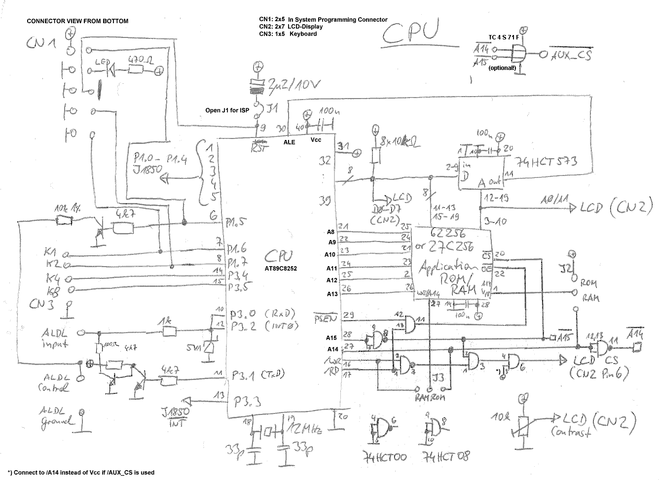
Well, what can I say about the circuit? First of all, note the ISP connector. You don't have to put it on the board, but if I ever decide to put new versions of ScanOS on the web for download, you can use this connector to program it into the CPU. If you use the ISP, open the solder bridge J1, or the reset capacitor will interfere with the programming dongle!
The four keyboard connector lines go to the keyboard assembly, and I didn't bother putting the details for the J1850 option on this already crowded piece of paper. Check the appropriate page if you're interested in that one.
I use a 5.1V Zener diode with a 1k resistor to protect the CPU's inputs from the ALDL voltages. The output can be pulled low by the two NPN transistors when using 8192 Baud communication.
On to the address decode circuitry. Both the 74HCT00 and 74HCT08 are SMT parts and are mounted under the CPU. This saves a lot of space, and the addressing is good enough for our purposes. /PSEN maps the application ROM/RAM into the entire 64K program address space, but only the upper 32K are used, because /CS is driven by the inverted A15 line. Similarly, if /RD goes low, the ROM/RAM is also selected. This way the memory appears in both address spaces of the CPU. If A15 is low (address range 0-$7FFF) the memory is automatically disabled. When a RAM is installed, the CPU's /WR signal is connected to the /WE input of the RAM. Since the pinout for RAM and ROM is slightly different, two jumpers (actually solder bridges) have to be set accordingly. The default is ROM, if you want RAM cut the two pads (J2 and J3) near the EPROM socket, and put solder bridges on the pads next to the cut ones. You'll find it.
The only other thing that's currently mapped into the address space is the LCD display. Because nothing else is needed, it gets a whopping 32K in the lower range. But there is space for a spare OR gate on the board, and with a little rewiring you can force the LCD into the lowest 16K, and get an additional Chipselect signal (/AUX_CS) for whatever purpose. The range for that one is then ($4000-$7FFF). Oh, the LCD display is one of those standard 16x2 displays with a 14 pin connector. There are a myriad variations out there, I hope yours is compatible with the standard.
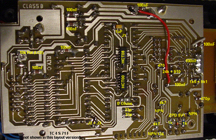
Other than that, I hope the schematics and picture will help you put the right parts in the right places. If not, drop me a note, and I'll try to clarify. Told ya this was an advanced project ;-)
Well, that's pretty much all there is to say about the circuit. When building FlexScan, you can measure that the crystal is oscillating, verify that Reset is initially high and then goes low, and you can check ALE to see if there is 1 MHz there. First try FlexScan without the J1850 option, without FlashStick, without an Application ROM or RAM and without the keyboard assembly. Power up, and you should see the welcome message on the LCD display. If you don't see that, check if there are (positive) CS pulses on the LCD's CS line. The SMT parts should be soldered in so that pin 7 is ground and pin 14 has 5 volts. Check if there are at least a few chip select pulses on the EPROM/RAM /CS line (only a few, so those may be hard to detect). Even without a keyboard you should be able to see that message. Check if you missed a wire bridge. Check if you connected the LCD correctly.
If you do see the message, continue with the keyboard. It should click if you hit a button. There is not much more to check until you write an application program to read the keyboard. Well, this should get you on the way. The more time you spend understanding (and debugging) the circuit, the more insights you'll get that will eventually help you when writing applications.
There have been
visitors to this site since May 31, 2000.